Milling PCB workflow
(experimental)
Using Eagle, Tracespace.io, InkScape and Fusion 360
- Make circuit and PCB layout in Autodesk Eagle (version 9.4.0)
File > Generate CAM data- Click OK. This will generate a zip archive with Gerber files (2D vector files used for PCB manufacturing).
- Unzip the .zip file and open the GerberFiles folder.
- Open https://tracespace.io/ to convert the desired Gerber files to SVG vector files.
- Open the desired .SVG files in Inkscape.
edit > select all(ctrl + a)object > ungroup(shift + ctrl + g)- the circles and squares are clones from hidden shapes. select one clone-object.
edit > select same > Object type(shift + alt + a)file > clone > unlink clone(shift + alt + d). The clone objects have now been changed to circle and rectangle objectsedit > select allpath > objects to pathpath > stroke to pathpath > break apartpath > union
- insert the SVG file in fusion 360
- set scale to
0,003779527597(The dimensions set in Eagle are correct in InkScape, but with scale set to 1, 1,27mm in eagle becomes 336,02083mm in Fusion 360) - select contours, extrude and configure setup and trace operation for milling
Bad SVG's
Circles

When circles are actually 4 arcs they won't be selectable for a bore or drill operation.
- Draw 2 construction lines between the 4 points of the bad circle.
- Draw a circle to measure the diameter of the bad circle. Note the dimension and cancel the circle.
- Delete the arc segments
- Draw a the new circle with the measured diameter
Arcs

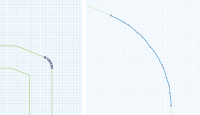
Some arcs are composed of multiple smaller arcs.
- Select all the segments by dragging the selection box from left to right. Only the line elements that are fully inside of the selection box are selected.
- Delete them
- Add a tangent arc
Engrave toolpath
If traces come close together, the tool will lift, cutting a thinner trace. This allows to set a relatively deep trace over-all to accommodate flex in the PCB substrate.
- Add an engrave toolpath strategy and select the traces. You don't need to select the holes yet, but make sure to select a contour line around all the traces. That way Fusion knows at which side of the lines the tool need to be placed. I tested 0.3mm depth, but 0,2mm or shallower should work better.


Here you can see the cut is made on the outside of the traces.
Small holes
- Put one of the PCB drills from the Hyrel kit in a 1/8“ (3.175mm) collet.
- No need to ad these to the tool list in Fusion. Simulate them with a 1mm flat endmill.
- Take the CAM profile “PCB-Drill” from CAM Templates > PCB. This plunges the drill straight down. As it does not helix, the hole is the same diameter as the drill.


